STM32F107VC/System architecture
The STM32F107VC is a highly complex device. To understand the device it's necessary first to understand the basic system architecture. Se Chapter 3 in the Reference Manual.
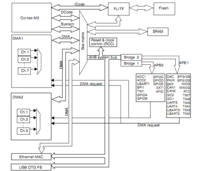
The STM32F107VC is a connectivity line device with the basic architecture shown to the right.
- Five masters:
- Cortex™-M3 core
- DCode bus (D-bus)
- System bus (S-bus)
- GP-DMA1 & 2 (general-purpose DMA)
- Ethernet DMA
- Three slaves:
- Internal SRAM
- Internal Flash memory
- AHB to APB bridges (AHB to APBx), which connect all the APB peripherals
ICode bus
This bus connects the Instruction bus of the Cortex™-M3 core to the Flash memory instruction interface. Prefetching is performed on this bus.
DCode bus
This bus connects the DCode bus (literal load and debug access) of the Cortex™-M3 core to the Flash memory Data interface.
System bus
This bus connects the system bus of the Cortex™-M3 core (peripherals bus) to a BusMatrix which manages the arbitration between the core and the DMA.
DMA bus
This bus connects the AHB master interface of the DMA to the BusMatrix which manages the access of CPU DCode and DMA to SRAM, Flash memory and peripherals.
BusMatrix
The BusMatrix manages the access arbitration between the core system bus and the DMA master bus. The arbitration uses a Round Robin algorithm. In connectivity line devices, the BusMatrix is composed of five masters (CPU DCode, System bus, Ethernet DMA, DMA1 and DMA2 bus) and three slaves (FLITF, SRAM and AHB2APB bridges). In other devices, the BusMatrix is composed of four masters (CPU DCode, System bus, DMA1 bus and DMA2 bus) and four slaves (FLITF, SRAM, FSMC and AHB2APB bridges).
AHB peripherals are connected on system bus through a BusMatrix to allow DMA access.
AHB/APB bridges (APB)
The two AHB/APB bridges provide full synchronous connections between the AHB and the 2 APB buses. APB1 is limited to 36 MHz, APB2 operates at full speed (up to 72 MHz depending on the device).
After each device reset, all peripheral clocks are disabled (except for the SRAM and FLITF). Before using a peripheral you have to enable its clock in the RCC_AHBENR, RCC_APB2ENR or RCC_APB1ENR register.
Note: When a 16- or 8-bit access is performed on an APB register, the access is transformed into a 32-bit access: the bridge duplicates the 16- or 8-bit data to feed the 32-bit vector.
