Difference between revisions of "STM32F107VC/GPIO"
m (→Default configuration) |
m (→MODE[1:0] configuratin bits) |
||
| (12 intermediate revisions by the same user not shown) | |||
| Line 22: | Line 22: | ||
==Port Bit Configuration== | ==Port Bit Configuration== | ||
Each bit can be configured using the configuration registers shown below | Each bit can be configured using the configuration registers shown below | ||
| − | {|border=1 ;style="margin: 0 auto; text-align: center;cellpadding="5" cellspacing="0" | + | ===GPIO Configuration Registers summary=== |
| − | |+ GPIO Configuration Registers. | + | {|border=1 ;style="margin: 0 auto; text-align: center;cellpadding="5" cellspacing="0" width=100% |
| + | |+ GPIO Configuration Registers. ('''Note:'''''x'' = Port A to G ) | ||
|- bgcolor=lightgrey | |- bgcolor=lightgrey | ||
| − | ! Name !! Function | + | ! Name !! [http://www.st.com/internet/com/TECHNICAL_RESOURCES/TECHNICAL_LITERATURE/REFERENCE_MANUAL/CD00171190.pdf Section] !! Name || r/w || Bits ||Function |
| + | |- | ||
| + | |[[/GPIOx_CRL|GPIO'''x'''_CRL]] || align=center | 9.2.1 || Port configuration register low || align=center | rw || CNF[1:0], MODE[1:0] ||Configure lowest 8 bit of port ''x''. IN or OUT | ||
| + | |- | ||
| + | |[[/GPIOx_CRH|GPIO'''x'''_CRH]] || align=center | 9.2.2 || Port configuration register high || align=center | rw ||CNF[1:0], MODE[1:0] ||Configure highest 8 bit of port ''x''. IN or OUT | ||
| + | |- | ||
| + | |[[/GPIOx_IDR|GPIO'''x'''_IDR]] || align=center | 9.2.3 || port input data register || align=center | r ||IDR[15:0] ||Read state of pins configured for input on port ''x'' (Lowest 16 bits of word) | ||
| + | |- | ||
| + | |[[/GPIOx_ODR|GPIO'''x'''_ODR]] || align=center | 9.2.4 || port output data register || align=center | rw || ODR[15:0]||Write to pins configured for Output on port ''x'' (Lowest 16 bits of word) | ||
|- | |- | ||
| − | | | + | |[[/GPIOx_BSRR|GPIO'''x'''_BSRR]] || align=center | 9.2.5 || Port bit set/reset register || align=center | w ||BS[15:0], BR[15:0] || Atomic Set/Reset individual Pins configured for Output. |
|- | |- | ||
| − | | | + | |[[/GPIOx_BRR|GPIO'''x'''_BRR]] || align=center | 9.2.6 || Port bit reset register || align=center | w ||BR[15:0] || Atomic Reset individual Pins configured for Output. (Lowest 16 bits of word) |
|- | |- | ||
| + | |[[/GPIOx_LCKR|GPIO'''x'''_LCKR]] || align=center | 9.2.7 || Port configuration lock register || align=center | rw ||LCK[15:0], LCKK|| Lock individual pins of port ''x'' (Freeze CRL and CRH of ports) | ||
|} | |} | ||
| + | ===Port bit Configuration summary=== | ||
{|border=1 ;style="margin: 0 auto; text-align: center;cellpadding="5" cellspacing="0" | {|border=1 ;style="margin: 0 auto; text-align: center;cellpadding="5" cellspacing="0" | ||
|+ Port bit configuration table | |+ Port bit configuration table | ||
| Line 38: | Line 49: | ||
! colspan=2 |Configuration mode !! CNF1 !! CNF0 !! MODE1 !! MODE0 !! PxODR register | ! colspan=2 |Configuration mode !! CNF1 !! CNF0 !! MODE1 !! MODE0 !! PxODR register | ||
|- align=center | |- align=center | ||
| − | |rowspan=2 |General Purpose Output ||Push-Pull||rowspan=2; |0||0||rowspan=4; colspan=2| | + | |rowspan=2 align=left|General Purpose Output || align=left |Push-Pull||rowspan=2; |0||0||rowspan=4; colspan=2|01<br/>10<br/>11<br/>See Mode below|| 0 or 1 |
| + | |- align=center | ||
| + | | align=left |Open Drain ||1|| 0 or 1 | ||
| + | |- align=center | ||
| + | |rowspan=2 align=left |Alternate function Output || align=left |Push-Pull||rowspan=2; |1||0|| Don't Care | ||
| + | |- align=center | ||
| + | | align=left |Open Drain ||1|| Don't Care | ||
| + | |- align=center | ||
| + | |rowspan=4 align=left |Input || align=left |Analog||rowspan=2; |0||0||rowspan=4; colspan=2|00|| Don't Care | ||
| + | |- align=center | ||
| + | | align=left |Input Floating|| 1 || Don't Care | ||
| + | |- align=center | ||
| + | | align=left |Input Pull-Down|| rowspan=2 | 1 || rowspan=2 | 0 || 0 | ||
| + | |- align=center | ||
| + | | align=left |Input Pull-Up|| 1 | ||
|- | |- | ||
| − | | | + | |} |
| + | ====MODE[1:0] configuration bits==== | ||
| + | {|border=1 ;style="margin: 0 auto; text-align: center;cellpadding="5" cellspacing="0" | ||
| + | |+ Output MODE bits. | ||
| + | |- bgcolor=lightgrey | ||
| + | ! MODE[1:0] !! Meaning | ||
| + | |- align=center | ||
| + | |00 ||align=left |Reserved | ||
| + | |- align=center | ||
| + | |01 ||align=left |Max. output speed 10 MHz | ||
| + | |- align=center | ||
| + | |10 ||align=left |Max. output speed 2 MHz | ||
| + | |- align=center | ||
| + | |11 ||align=left |Max. output speed 50 MHz | ||
|- | |- | ||
| − | |||
|} | |} | ||
==Detailed description== | ==Detailed description== | ||
| − | For detailed description see [http://www.st.com/internet/com/TECHNICAL_RESOURCES/TECHNICAL_LITERATURE/REFERENCE_MANUAL/CD00171190.pdf STM32F107VC Reference Manual] Chapter 9. | + | For detailed description of GPIO see [http://www.st.com/internet/com/TECHNICAL_RESOURCES/TECHNICAL_LITERATURE/REFERENCE_MANUAL/CD00171190.pdf STM32F107VC Reference Manual] Chapter 9. |
[[Category:ARM]] | [[Category:ARM]] | ||
Latest revision as of 08:17, 15 November 2011
General Purpose and Alternate Function I/O
GPIO functional description
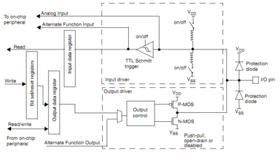
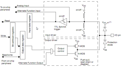
Each of the general-purpose I/O ports has two 32-bit configuration registers (GPIOx_CRL, GPIOx_CRH), two 32-bit data registers (GPIOx_IDR, GPIOx_ODR), a 32-bit set/reset register (GPIOx_BSRR), a 16-bit reset register (GPIOx_BRR) and a 32-bit locking register (GPIOx_LCKR).
Subject to the specific hardware characteristics of each I/O port listed in the datasheet, each port bit of the General Purpose IO (GPIO) Ports, can be individually configured by software in several modes:
- Input floating
- Input pull-up
- Input-pull-down
- Analog
- Output open-drain
- Output push-pull
- Alternate function push-pull
- Alternate function open-drain
Each I/O port bit is freely programmable, however the I/O port registers have to be accessed as 32-bit words (half-word or byte accesses are not allowed). The purpose of the GPIOx_BSRR and GPIOx_BRR registers is to allow atomic read/modify accesses to any of the GPIO registers. This way, there is no risk that an IRQ occurs between the read and the modify access.
Default configuration
During and just after reset, the alternate functions are not active and the I/O ports are configured in Input Floating mode.
Port Bit Configuration
Each bit can be configured using the configuration registers shown below
GPIO Configuration Registers summary
| Name | Section | Name | r/w | Bits | Function |
|---|---|---|---|---|---|
| GPIOx_CRL | 9.2.1 | Port configuration register low | rw | CNF[1:0], MODE[1:0] | Configure lowest 8 bit of port x. IN or OUT |
| GPIOx_CRH | 9.2.2 | Port configuration register high | rw | CNF[1:0], MODE[1:0] | Configure highest 8 bit of port x. IN or OUT |
| GPIOx_IDR | 9.2.3 | port input data register | r | IDR[15:0] | Read state of pins configured for input on port x (Lowest 16 bits of word) |
| GPIOx_ODR | 9.2.4 | port output data register | rw | ODR[15:0] | Write to pins configured for Output on port x (Lowest 16 bits of word) |
| GPIOx_BSRR | 9.2.5 | Port bit set/reset register | w | BS[15:0], BR[15:0] | Atomic Set/Reset individual Pins configured for Output. |
| GPIOx_BRR | 9.2.6 | Port bit reset register | w | BR[15:0] | Atomic Reset individual Pins configured for Output. (Lowest 16 bits of word) |
| GPIOx_LCKR | 9.2.7 | Port configuration lock register | rw | LCK[15:0], LCKK | Lock individual pins of port x (Freeze CRL and CRH of ports) |
Port bit Configuration summary
| Configuration mode | CNF1 | CNF0 | MODE1 | MODE0 | PxODR register | |
|---|---|---|---|---|---|---|
| General Purpose Output | Push-Pull | 0 | 0 | 01 10 11 See Mode below |
0 or 1 | |
| Open Drain | 1 | 0 or 1 | ||||
| Alternate function Output | Push-Pull | 1 | 0 | Don't Care | ||
| Open Drain | 1 | Don't Care | ||||
| Input | Analog | 0 | 0 | 00 | Don't Care | |
| Input Floating | 1 | Don't Care | ||||
| Input Pull-Down | 1 | 0 | 0 | |||
| Input Pull-Up | 1 | |||||
MODE[1:0] configuration bits
| MODE[1:0] | Meaning |
|---|---|
| 00 | Reserved |
| 01 | Max. output speed 10 MHz |
| 10 | Max. output speed 2 MHz |
| 11 | Max. output speed 50 MHz |
Detailed description
For detailed description of GPIO see STM32F107VC Reference Manual Chapter 9.

