Difference between revisions of "STM32F107VC/System architecture"
From Teknologisk videncenter
m (Created page with "The STM32F107VC is a highly complex device. To understand the device it's necessary first to understand the basic system architecture. Se Chapter 3 in the [http://www.st.com/...") |
m |
||
| Line 1: | Line 1: | ||
The [[STM32F107VC]] is a highly complex device. To understand the device it's necessary first to understand the basic system architecture. Se Chapter 3 in the [http://www.st.com/internet/com/TECHNICAL_RESOURCES/TECHNICAL_LITERATURE/REFERENCE_MANUAL/CD00171190.pdf Reference Manual]. | The [[STM32F107VC]] is a highly complex device. To understand the device it's necessary first to understand the basic system architecture. Se Chapter 3 in the [http://www.st.com/internet/com/TECHNICAL_RESOURCES/TECHNICAL_LITERATURE/REFERENCE_MANUAL/CD00171190.pdf Reference Manual]. | ||
| − | + | [[Image:STM32F107VC system.png|right|300px|thumb|STM32F107VC System Architecture (Click to enlarge)]] | |
The [[STM32F107VC]] is a ''connectivity line device'' with the basic architecture shown to the right. | The [[STM32F107VC]] is a ''connectivity line device'' with the basic architecture shown to the right. | ||
* Five masters: | * Five masters: | ||
Revision as of 07:07, 3 September 2011
The STM32F107VC is a highly complex device. To understand the device it's necessary first to understand the basic system architecture. Se Chapter 3 in the Reference Manual.
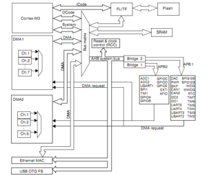
The STM32F107VC is a connectivity line device with the basic architecture shown to the right.
- Five masters:
- Cortex™-M3 core DCode bus (D-bus) and System bus (S-bus)
- GP-DMA1 & 2 (general-purpose DMA)
- Ethernet DMA
- Three slaves:
- Internal SRAM
- Internal Flash memory
- AHB to APB bridges (AHB to APBx), which connect all the APB peripherals
