Difference between revisions of "STM32F107VC/RCC/Clock Modes example"
From Teknologisk videncenter
< STM32F107VC | RCC
m (→Configuring Clock mode 5) |
|
(No difference)
| |
Latest revision as of 14:16, 27 January 2012
Clock mode 1
Configuring clock mode 1
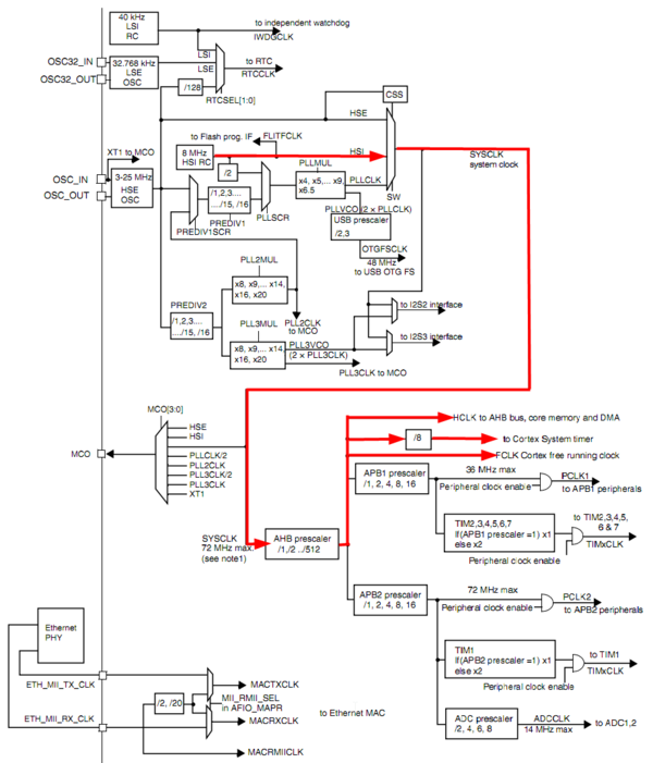
If the controller is using the HSE clock, and you want to shift to HSI direct clocking.
/* sub rcc_clockmode1()
   abstract: Select default as System Clock (HSI 8 Mhz)

   input...:  -

   output..: -
   limits..: No errorcheck performed
   *********************************************
   See: http://mars.tekkom.dk/mediawiki/index.php/STM32F107VC/RSS/Clock_Paths
        http://mars.tekkom.dk/mediawiki/index.php/STM32F107VC/RSS
   *********************************************
   Step 1: Enabling the HSI clock - RCC_CR bit (If not enabled)
  		   HSION = 1 HSI : oscillator on
   Step 2: Waiting until HSI clock is ready an can be used as Clock Source
           RCC_CR bit HSIRDY = 0 : Oscillator Not Ready
		   RCC_CR bit HSIRDY = 1 : Oscillator Ready
   Step 3: Select HSI in SW[1:0] as Clock Source
           RCC_CFGR bits SW[1:0] = 00 : HSI selected
   Step 4: Select AHB prescaler=1
           RCC_CFGR bits HPRE[3:0] = 0000
   Step 5: Setting FLASH wait states FLASH_ACR bits LATENCY[2:0] to 0 Wáit States(section 3.3)
  		   LATECY[2:0] = 000 - Zero wait state. ( 0 Hz  < SYSCLK <= 24 Mhz)
  		   LATECY[2:0] = 001 - One wait state.  (24 MHz < SYSCLK <= 48 Mhz)
  		   LATECY[2:0] = 010 - Two wait state.  (48 MHz < SYSCLK <= 72 Mhz)
   Step 6: Disabling HSE Clock- RCC_CR bit
  		   HSEON = 0 : oscillator off
*/
void rcc_clockmode1( void ) {
  	// Step 1 - Enabling the HSI clock - If not enabled and ready
	if ( (RCC->CR & RCC_CR_HSIRDY) == 0) {
 	  RCC->CR |= RCC_CR_HSION;  // HSION=1

	  //Step 2 - Waiting until HSI clock is ready
	  while ((RCC->CR & RCC_CR_HSIRDY) == 0) {}; // Wait HSIRDY = 1
	}
	//Step 3: Select HSI in SW[1:0] as Clock Source
	//         Take care. SW[1:0] Select the clock source
	RCC->CFGR &= 0xfffffffc;

	//Step 4: Select AHB prescaler=1
	RCC->CFGR &= 0xffffff0f; // HPRE[3:0] = 0000

    //Step 5: Setting FLASH wait states FLASH_ACR bits LATENCY[2:0] to 0 Wáit
	FLASH->ACR &= 0xfffffff8; //LATENCY[2:0] = 000

	//Step 6: Disabling HSE Clock- RCC_CR bit
	RCC->CR &= ~RCC_CR_HSEON;

}
Clock mode 5
Configuring Clock mode 5
/* sub rcc_clockmode5()
   abstract: Select HSE as System Clock with,
     Crystal = 25 MHz
	 SYSCLK  = 72 MHz
	 FCLK    = 72 MHz
	 OTGFSCLK= 48 MHz (USB)

   input...:  -

   output..: -
   limits..: No errorcheck performed
   *********************************************
   See: http://mars.tekkom.dk/mediawiki/index.php/STM32F107VC/RSS/Clock_Paths
        http://mars.tekkom.dk/mediawiki/index.php/STM32F107VC/RSS
   *********************************************

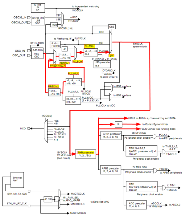
   To select the frequencies 72 MHz as SYSCLK from 25 MHz Crystal the
   following calculation is necesary 25 MHz / 5 * 16 / 10 * 9 = 72 MHz

   PREDIV2 - Divide by 5
   PLL2MUL - Multiply by 16
   PREDIV1 - Divide by 10
   PLLMUL  - Multiply by 9

   Step  0: HSEBYP default = 0 (Using Crystral = default)
   Step  1: Shift to Clockmode=1 (Freeing the Clock Path for programming)
   Step  2: Enabling the HSE clock - RCC_CR bit
  		   HSION = 1 HSE : oscillator on
   Step  3: Waiting until HSE clock is ready an can be used as Clock Source
           RCC_CR bit HSERDY = 0 : Oscillator Not Ready
		   RCC_CR bit HSERDY = 1 : Oscillator Ready
   Step  4: Select RCC_CFGR2 PREDIV2[3:0] divide by 5 =  0100
   Step  5: Disable RCC_CR PLL2ON = Disable (Shut down PLL2MUL)
   Step  6: Select RCC_CFGR2 PLL2MUL[3:0] multiply by 16 = 1110
   Step  7: Enable RCC_CR PLL2ON = Enable (Start pll2MUL after programmed)
   Step  8: Wait for PLL2MUL to lock RCC_CR bit PLL2RDY = 1
   Step  9: Select PLL2MUL as PREDIV1SRC - RCC_CFGR2 bit PREDIV1SRC = 1
   Step 10: Select RCC_CFGR2 PREDIV1[3:0] divide by 10 = 1001
   Step 11: Select PREDIV1 as PLLSRC - RCC_CFGR bit PLLSRC = 1
   Step 12: Disable RCC_CR bit PLLON = 0
   Step 13: Select RCC_CFGR PLLMUL[3:0] multiply by 9 = 0111
   Step 14: Enable RCC_CR bit PLLON = 1
   Step 15: Wait for PLLMUL to lock RCC_CR bit PLLRDY = 1
   Step 16: USB Prescaler divide by 3 ( 72 Mhz * 2 / 3 )  = 48 MHz
            RCC_CFGR bit OTGFSPRE = 0
   Step 17: Select AHB prescaler=1 - RCC_CFGR bits HPRE[3:0] = 0000
   Step 18: Enable prefetch FLASH_ACR bit PRFTBE = 1
   Step 19: Setting FLASH wait states FLASH_ACR bits LATENCY[2:0] to 2 Wáit States(section 3.3)
  		    LATECY[2:0] = 000 - Zero wait state. ( 0 Hz  < SYSCLK <= 24 Mhz)
  		    LATECY[2:0] = 001 - One wait state.  (24 MHz < SYSCLK <= 48 Mhz)
  		    LATECY[2:0] = 010 - Two wait state.  (48 MHz < SYSCLK <= 72 Mhz)
   Step 20: RCC_CFGR bits PPRE1[2:0] = 100 -APB1 Prescaler divide by 2 = 36 MHz
   Step 21: RCC_CFGR bits ADCPRE[1:0] = 10 ADC-prescaler divide by 6 72 MHz / 6 = 12 MHz
   Step 22: Select PLLCLK in SW[1:0] as Clock Source
            RCC_CR SW[1:0] = 10
   Step 23: Disabling HSI Clock- RCC_CR bit
  		   HSION = 0 : oscillator off
           RCC_CFGR bits SW[1:0] = 00 : HSI selected
*/
void rcc_clockmode5( void ) {
int i;
	//Step  1: Shift to Clockmode=1
	rcc_clockmode1();

	// Step 2 - Enabling the HSE clock
 	RCC->CR |= RCC_CR_HSEON;  // HSEON=1

	//Step 3 - Waiting until HSE clock is ready
	while ((RCC->CR & RCC_CR_HSERDY) == 0) {}; // Wait HSERDY = 1

	//Step  4: Select RCC_CFGR2 PREDIV2[3:0] divide by 5 =  0100 (bits[7:4])
	RCC->CFGR2 |= 0x00000040; // Setting bit x1xx
	RCC->CFGR2 &= 0xffffff4f; // Resetting bit 0x00

    //Step  5: Disable RCC_CR PLL2ON = Disable (Shut down PLL2MUL)
	RCC->CR &= ~( 1 << 26 ); // Resetting bit 26 disabling PPL2MUL

	//Step  6: Select RCC_CFGR2 PLL2MUL[3:0] multiply by 16 = 1110 (bits[11:8])
	RCC->CFGR2 |= 0x00000e00; // Setting bits 111x
	RCC->CFGR2 &= 0xfffffeff; // Resetting bit xxx0

	//Step  7: Enable RCC_CR PLL2ON = Enable (Start pll2MUL after programmed)
	RCC->CR |=  1 << 26 ; // Setting bit 26 enabling PPL2MUL

	//Step  8: Wait for PLL2MUL to lock RCC_CR bit PLL2RDY = 1
	while ((RCC->CR & RCC_CR_PLL2RDY) == 0) {}; // Wait PLL2RDY = 1

	//Step  9: Select PLL2MUL as PREDIV1SRC - RCC_CFGR2 bit PREDIV1SRC = 1
	RCC->CFGR2 |= 1 << 16; // Setting bit 16 selecting PLL2MUL

	//Step 10: Select RCC_CFGR2 PREDIV1[3:0] divide by 10 = 1001 (bits[3:0])
	RCC->CFGR2 |= 0x00000009; // Setting bits 1xx1
	RCC->CFGR2 &= 0xfffffff9; // Resetting bit x00x

	//Step 11: Select PREDIV1 as PLLSRC - RCC_CFGR bit PLLSRC = 1
	RCC->CFGR |= RCC_CFGR_PLLSRC;

	//Step 12: Disable RCC_CR bit PLLON = 0
	RCC->CR &= ~( 1 << 24 ); // Resetting bit 24 disabling PPLMUL

	//Step 13: Select RCC_CFGR PLLMUL[3:0] multiply by 9 = 0111	(bits[21:18])
	RCC->CFGR &= ~( 1 << 21 ); // Bit 21 = 0
	RCC->CFGR |= 1 << 20; 		// bit 20 = 1
	RCC->CFGR |= 1 << 19; 		// bit 19 = 1
	RCC->CFGR |= 1 << 18; 		// bit 18 = 1

	//Step 14: Enable RCC_CR bit PLLON = 1
	RCC->CR |=  1 << 24 ; // Setting bit 24 enabling PPLMUL

	//Step 15: Wait for PLLMUL to lock RCC_CR bit PLLRDY = 1
	while ((RCC->CR & RCC_CR_PLL1RDY) == 0) {}; // Wait PLL1RDY = 1

	//Step 16: USB Prescaler divide by 3 ( 72 Mhz * 2 / 3 )  = 48 MHz
	RCC->CFGR &= ~(1 << 22); //Resetting OTGFSPRE selects divide by 3

	//Step 17: Select AHB prescaler=1 - RCC_CFGR bits HPRE[3:0] = 0000 (bits[7:4])
	RCC->CFGR2 &= 0xffffff0f; // Resetting bit 0000

	//Step 18: Enable prefetch FLASH_ACR bit PRFTBE = 1
	FLASH->ACR |= 1 << 4;

	//Step 19: Setting FLASH wait states FLASH_ACR bits LATENCY[2:0] to 2 Wáit States(section 3.3)
	FLASH->ACR |= 0x00000002;
	FLASH->ACR &= 0xfffffffa;

	for(i=0;i < 100000;i++);

	//Step 20: RCC_CFGR bits PPRE1[2:0] = 100 -APB1 Prescaler divide by 2 = 36 MHz
	rcc_cfgr( 0x00000300, 0 ); //Set PPRE1[1:0] = 0
	rcc_cfgr( 0x00000400, 1 ); //Set PPRE1[2] = 1

	//Step 21: RCC_CFGR bits PPRE1[2:0] = 100 -APB1 Prescaler divide by 2 = 36 MHz
	rcc_cfgr( 1 << 14, 0 ); //Set ADCPRE[0] = 0
	rcc_cfgr( 1 << 15, 1 ); //Set ADCPRE[1] = 1

	//Step 22: Select PLLCLK in SW[1:0] as Clock Source
	RCC->CFGR |= RCC_CFGR_PLLON;

   //Step 23 - Disable HSI
	RCC->CR &= ~RCC_CR_HSION;
}
}

