GPS RECEIVER - MT3329
From Teknologisk videncenter
Contents
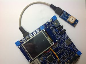
Module on MCBSTM32C Keil board
Using the STM32F107VC remapped USART1 to PB6 (USART1_TX)and PB7 (USART1_RX). The GPS module uses VCC and GND and not RS232 levels on TX/RX. Five boards are modified for the five GPS modules bought.
- The [1] show that PB6 is used for CAN2 bus TX. CAN2 bus can't be used at the same time as the GPS module.
- The [2] show that PB7 is used for the USER button. To use PB7 as RX from the GPS module it is necessary to remove C20. The USER switch can't be used at the same time as the GPS module.
Connections
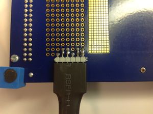
Solder a 6 pin 0,1 inch 90 degrees angle. See picture 2 and connect
- Pin 1 to 3,3V (Red wire)
- Pin 2 to GND (Black wire)
- Pin 3 - Not used in this project ( 1 second pulse signal from GPS module )
- Pin 4 to PB7 (Orange wire) - GPS module TX
- Pin 5 to PB6 (Yellow wire) - GPS module RX
- Pin 6 - NOt used in this project ( FIX signal )
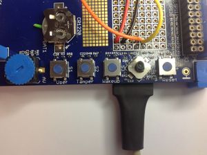
Battery connector on keil board
The minus pole on the battery has no electrical connection to the main board. To make a connection a desisolated wire was placed between the minuspole on the battery and the goldplated area on the PCB under the battery. See picture 2.
USART 1 code
To communicate with the GPS module the following code gives access to USART 1.
- NOTE
- The example below is a codesnippet from the test code. The usart1_rx function should be called from an RTX thread called t_gps.
- This is only test software. No buffer to hold unread data
USART1
CLOCK = PCLK1 AFTER APB1 PRESCALER

BaudRate =   fck / ( 16 * USARTDIV )

Fx:
  fck = 72 Mhz
  Wanted BuadRate = 9.600

  USARTDIV = fck/ (16 * BaudRate ) =
    72000000/ (16 * 9600) = 468,75

	Mantissa = 438 - as hex = 0x1D4
	Fraction = 16*0.75 = 6 - as hex 0xC
*/
void usart1_enable( void) {
//Step  1: RCC_APB2ENR - Enable Clock for Port B
rcc_apb2enr(1 << 3,ENABLE);

//Step  2: RCC_CFGR bits PPRE1[2:0] = 100 -APB1 Prescaler divide by 2 = 36 MHz
rcc_cfgr( 0x00000300, 0 ); //Set PPRE1[1:0] = 0
rcc_cfgr( 0x00000400, 1 ); //Set PPRE1[2] = 1

//Step  3: RCC_APB2ENR - Enable AFIO Clock - Alternate Clock I/O Enable
rcc_apb2enr(1 << 0,ENABLE);

//Step  4: AFIO_MAPR - Remap USART1  to Port B
rcc_afio_mapr(1 << 2, ENABLE);

//Step 5.1 and 5.2 - Enable pin 7 as RX and pin 6 as TX
GPIOB->CRL &= 0x00FFFFFF;
GPIOB->CRL |= 0x4B000000;			   //Pin 7: 0100 Pin 6: 1011

//Step  6: RCC Enable USART in RCC_APB2ENR
rcc_apb2enr( 1 << 14, ENABLE); //set bit 14 in RCC_APB2ENR (Enable USART1)

//Step  7.1 and 7.2: USART_BRR bits DIV_Mantissa[11:0] = 0x1d4 and fraction = c
USART1->BRR = 0x01d4c;

//Step  8: USART_CR1 bit UE - Uart Enable = 1
USART1->CR1 |= 1 << 13;

//Step 13: USART_CR1 bit TE - Tranmitter enable = 1
USART1->CR1 |= 1 << 3;

//Step 14: USART_CR1 bit RE - Receiver enable = 1
USART1->CR1 |= 1 << 2;

//Step 15: USART_CR1 bit RXNEIE - Receiver interrupt enable = 1
USART1->CR1 |= 1 << 5;

}

void usart1_tx( char character ) {
	while ((USART1->SR & ( 1 << 6)) == 0) {}; // Wait HSERDY = 1
	USART1->DR = (uint16_t) character;
}
void putstr(char *string) {
	int i;
	for ( i=0; string[i] != 0; i++ ) {
		usart1_tx(string[i]);
	}
}

//Receive
char usart1_rx() {
	os_evt_wait_and (0x0001, 0xffff);
	return(USART1->DR);
}

void USART1_IRQHandler( void ) __irq {

	isr_evt_set(0x0001, t_gps);
	while ((USART1->SR & ( 1 << 5)) == 0) {}; // Wait RXNE = 1

}
Data sheets
ARM board projects


