Difference between revisions of "STM32F107VC/RCC"
From Teknologisk videncenter
m (Created page with "=RCC - reset and clock control = right|thumb|300px|Clock Tree (Click to enlarge) STM32F107VC is a Connectivity Line Device and this register refe...") |
m |
||
| Line 7: | Line 7: | ||
#Power Reset | #Power Reset | ||
#Backup Domain Reset | #Backup Domain Reset | ||
| − | === | + | Se section 8.1 of the [http://www.st.com/internet/com/TECHNICAL_RESOURCES/TECHNICAL_LITERATURE/REFERENCE_MANUAL/CD00171190.pdf The Reference manual] for further information. |
| + | ==Clocks== | ||
| + | Three different clock sources can be used to drive the system clock (SYSCLK): | ||
| + | *HSI oscillator clock | ||
| + | *HSE oscillator clock | ||
| + | *PLL clock | ||
| + | ===HSI - High Speed Internal Clock=== | ||
| + | The HSI clock signal is generated from an internal 8 MHz RC Oscillator and can be used | ||
| + | directly as a system clock or divided by 2 to be used as PLL input. | ||
| + | {|border=1 ;style="margin: 0 auto; text-align: center;cellpadding="5" cellspacing="0" width=100% | ||
| + | |+ RSS HSI Configuration Registers. | ||
| + | |- bgcolor=lightgrey | ||
| + | ! Name !! [http://www.st.com/internet/com/TECHNICAL_RESOURCES/TECHNICAL_LITERATURE/REFERENCE_MANUAL/CD00171190.pdf Section] !! Name || r/w || Bits ||Function | ||
| + | |- | ||
| + | |[[/RCC_RC|RCC_RC]] || align=center | 8.3.1 || Clock Control Register || align=center | rw/r || HSICAL[7:0],HSITRIM[4:0] HSIRDY,HSION ||HSI ON and calibration | ||
| + | |- | ||
| + | |} | ||
| + | ===HSE - High Speed External clock=== | ||
| + | The high speed external clock signal (HSE) can be generated from two possible clock | ||
| + | sources: | ||
| + | * HSE external crystal/ceramic resonator | ||
| + | *HSE user external clock | ||
| + | The [[MCBSTM32C]] evaluation board has a 25Mhz on board crystal for HSE Clock. | ||
| + | ===PLL - Phase Locked Loops=== | ||
| + | The main PLL provides a frequency multiplier starting from one of the following clock | ||
| + | sources: | ||
| + | *HSI clock divided by 2 | ||
| + | *HSE or PLL2 clock through a configurable divider | ||
__NOTOC__ | __NOTOC__ | ||
[[Category:ARM]] | [[Category:ARM]] | ||
Revision as of 13:06, 1 September 2011
RCC - reset and clock control
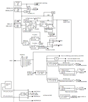
STM32F107VC is a Connectivity Line Device and this register refers to Chapter 8 in The Reference manual.
Reset
There are three tyoes of reset
- System Reset
- Power Reset
- Backup Domain Reset
Se section 8.1 of the The Reference manual for further information.
Clocks
Three different clock sources can be used to drive the system clock (SYSCLK):
- HSI oscillator clock
- HSE oscillator clock
- PLL clock
HSI - High Speed Internal Clock
The HSI clock signal is generated from an internal 8 MHz RC Oscillator and can be used directly as a system clock or divided by 2 to be used as PLL input.
| Name | Section | Name | r/w | Bits | Function |
|---|---|---|---|---|---|
| RCC_RC | 8.3.1 | Clock Control Register | rw/r | HSICAL[7:0],HSITRIM[4:0] HSIRDY,HSION | HSI ON and calibration |
HSE - High Speed External clock
The high speed external clock signal (HSE) can be generated from two possible clock sources:
- HSE external crystal/ceramic resonator
- HSE user external clock
The MCBSTM32C evaluation board has a 25Mhz on board crystal for HSE Clock.
PLL - Phase Locked Loops
The main PLL provides a frequency multiplier starting from one of the following clock sources:
- HSI clock divided by 2
- HSE or PLL2 clock through a configurable divider
